- 您現(xiàn)在的位置:買賣IC網(wǎng) > PDF目錄45010 > M30100F3TFP 16-BIT, FLASH, 16 MHz, MICROCONTROLLER, PQFP32 PDF資料下載
參數(shù)資料
| 型號: | M30100F3TFP |
| 元件分類: | 微控制器/微處理器 |
| 英文描述: | 16-BIT, FLASH, 16 MHz, MICROCONTROLLER, PQFP32 |
| 封裝: | PLASTIC, LQFP-32 |
| 文件頁數(shù): | 3/163頁 |
| 文件大小: | 2767K |
| 代理商: | M30100F3TFP |
第1頁第2頁當(dāng)前第3頁第4頁第5頁第6頁第7頁第8頁第9頁第10頁第11頁第12頁第13頁第14頁第15頁第16頁第17頁第18頁第19頁第20頁第21頁第22頁第23頁第24頁第25頁第26頁第27頁第28頁第29頁第30頁第31頁第32頁第33頁第34頁第35頁第36頁第37頁第38頁第39頁第40頁第41頁第42頁第43頁第44頁第45頁第46頁第47頁第48頁第49頁第50頁第51頁第52頁第53頁第54頁第55頁第56頁第57頁第58頁第59頁第60頁第61頁第62頁第63頁第64頁第65頁第66頁第67頁第68頁第69頁第70頁第71頁第72頁第73頁第74頁第75頁第76頁第77頁第78頁第79頁第80頁第81頁第82頁第83頁第84頁第85頁第86頁第87頁第88頁第89頁第90頁第91頁第92頁第93頁第94頁第95頁第96頁第97頁第98頁第99頁第100頁第101頁第102頁第103頁第104頁第105頁第106頁第107頁第108頁第109頁第110頁第111頁第112頁第113頁第114頁第115頁第116頁第117頁第118頁第119頁第120頁第121頁第122頁第123頁第124頁第125頁第126頁第127頁第128頁第129頁第130頁第131頁第132頁第133頁第134頁第135頁第136頁第137頁第138頁第139頁第140頁第141頁第142頁第143頁第144頁第145頁第146頁第147頁第148頁第149頁第150頁第151頁第152頁第153頁第154頁第155頁第156頁第157頁第158頁第159頁第160頁第161頁第162頁第163頁
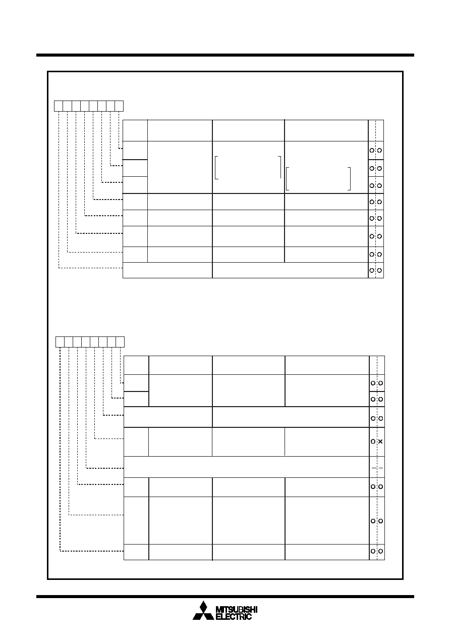
Serial I/O
Under
development
Tentative Specifications REV.E1
Specifications in this manual are tentative and subject to change.
Mitsubishi microcomputers
M30100/M30102 Group
SINGLE-CHIP 16-BIT CMOS MICROCOMPUTER
100
UARTi transmit/receive mode register
Symbol
Address
When reset
UiMR(i=0,1)
00A016, 00A816
0016
b7 b6
b5
b4
b3
b2
b1 b0
Bit name
Bit
symbol
W
R
Must be fixed to 001
0 0 0 : Serial I/O invalid
0 1 0 : Inhibited
0 1 1 : Inhibited
1 1 1 : Inhibited
b2 b1 b0
CKDIR
SMD1
SMD0
Serial I/O mode select bit
SMD2
Internal/external clock
select bit
STPS
PRY
PRYE
Parity enable bit
0 : Internal clock
1 : External clock
Stop bit length select bit
Odd/even parity select bit
0 : One stop bit
1 : Two stop bits
0 : Parity disabled
1 : Parity enabled
1 0 0 : Transfer data 7 bits long
1 0 1 : Transfer data 8 bits long
1 1 0 : Transfer data 9 bits long
0 0 0 : Serial I/O invalid
0 1 0 : Inhibited
0 1 1 : Inhibited
1 1 1 : Inhibited
b2 b1 b0
0 : Internal clock
1 : External clock
Invalid
Valid when bit 6 = “1”
0 : Odd parity
1 : Even parity
Invalid
Function
(During UART mode)
Function
(During clock synchronous
serial I/O mode)
UARTi transmit/receive control register 0
Symbol
Address
When reset
UiC0(i=0,1)
00A416, 00AC16
0816
b7
b6
b5
b4
b3
b2 b1
b0
Function
(During UART mode)
W
R
Function (Note)
(During clock synchronous
serial I/O mode)
TXEPT
CLK1
CLK0
NCH
CKPOL
BRG count source
select bit
Transmit register empty
flag
0 : Transmit data is output at
falling edge of transfer clock
and receive data is input at
rising edge
1 : Transmit data is output at
rising edge of transfer clock
and receive data is input at
falling edge
CLK polarity select bit
Data output select bit
0 0 : f1 is selected
0 1 : f8 is selected
1 0 : f32 is selected
1 1 : fc is selected
b1 b0
0 : LSB first
1 : MSB first
0 : Data present in transmit
register (during transmission)
1 : No data present in transmit
register (transmission
completed)
0 : TXDi pin is CMOS output
1 : TXDi pin is N-channel
open-drain output
UFORM Transfer format select bit
0 0 : f1 is selected
0 1 : f8 is selected
1 0 : f32 is selected
1 1 : fc is selected
b1 b0
0 : Data present in transmit register
(during transmission)
1 : No data present in transmit
register (transmission completed)
0: TXDi pin is CMOS output
1: TXDi pin is N-channel
open-drain output
Must always be “0”
Bit name
Bit
symbol
Must always be “0”
O
Must set to "0".
(Note)
Note: Set the corresponding port direction register to “0”.
0
Reserved bit
Nothing is assigned.
In an attempt to write to this bit, write "0". The value, if read, turns out to be "0".
Reserved bit
Must always be set to “0”
Figure 1.15.4. Serial I/O-related registers (2)
相關(guān)PDF資料 |
PDF描述 |
|---|---|
| M30102M2T-XXXFP | 16-BIT, MROM, 16 MHz, MICROCONTROLLER, PQFP48 |
| M30100M2T-XXXFP | 16-BIT, MROM, 16 MHz, MICROCONTROLLER, PQFP32 |
| M30102M6T-XXXFP | 16-BIT, MROM, 16 MHz, MICROCONTROLLER, PQFP48 |
| M30102M3-XXXFP | 16-BIT, MROM, 16 MHz, MICROCONTROLLER, PQFP48 |
| M30100M2T-XXXFP | 16-BIT, MROM, 16 MHz, MICROCONTROLLER, PQFP32 |
相關(guān)代理商/技術(shù)參數(shù) |
參數(shù)描述 |
|---|---|
| M30100T3-RPD-E | 制造商:Renesas Electronics Corporation 功能描述:DEV EMULATOR POD M16C/10 SERIES - Bulk |
| M30100T-PTC | 制造商:RENESAS 制造商全稱:Renesas Technology Corp 功能描述:Converter for Connecting 32-pin 0.8mm-pitch QFP for M30100T-PRB (for M16C/10 Group M30100) |
| M30-1010046 | 功能描述:集管和線殼 1.25MM FEMALE CRIMP TIN PK OF 105 RoHS:否 產(chǎn)品種類:1.0MM Rectangular Connectors 產(chǎn)品類型:Headers - Pin Strip 系列:DF50 觸點類型:Pin (Male) 節(jié)距:1 mm 位置/觸點數(shù)量:16 排數(shù):1 安裝風(fēng)格:SMD/SMT 安裝角:Right 端接類型:Solder 外殼材料:Liquid Crystal Polymer (LCP) 觸點材料:Brass 觸點電鍍:Gold 制造商:Hirose Connector |
| M3010102636207.32LLZZ | 制造商:3M Electronic Products Division 功能描述:QUOTE # V05-0068 |
| M30102 | 制造商:RENESAS 制造商全稱:Renesas Technology Corp 功能描述:SINGLE-CHIP 16-BIT CMOS MICROCOMPUTER |
發(fā)布緊急采購,3分鐘左右您將得到回復(fù)。